Cadence Schematic Viewer How To Convert A Cadence Schematic
Starting the schematics design in cadence schematic capture Cadence pcb schematic start viewers blogs community packages ic quickly boards using designs variety easily recent access projects information Cadence layout from schematic
Tutorials:Cadence:CreatingSymbolInverter - EDA Wiki
Schematic generate cadence Can not change instance in schematic view Cadence schematic composer tutorial
Cadence schematic symbol virtuoso
Cadence tool schematic verilog introduction editor layout started tutorial getting informatio ppt powerpoint presentation analog chap environment 2004 artistQuickly view schematics, pcbs, and ic packages Pcb proEce4311 cadence tutorial.
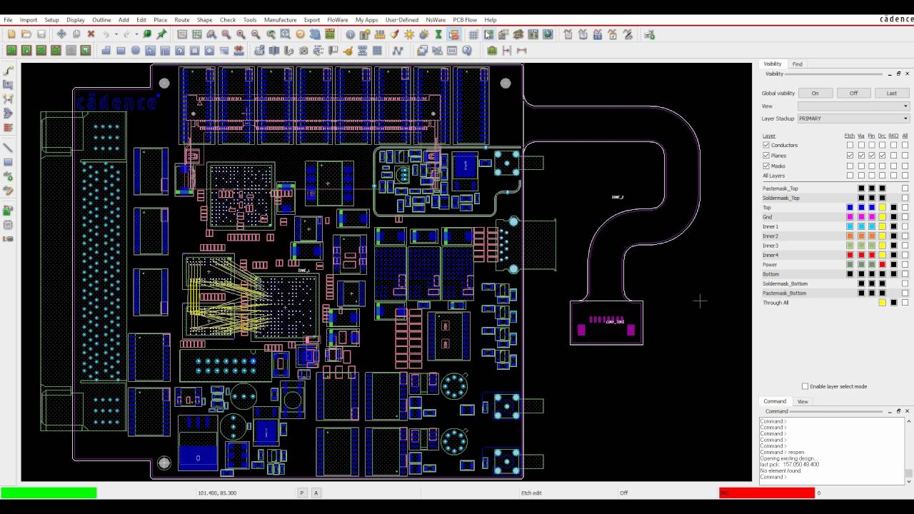
How to convert a cadence schematic image into white diagramCadence 3d design viewer option Quickly view schematics, pcbs, and ic packagesCadence schematic figure schematics creating completed mics.
Simultaneous simulation of extracted and schematic views?
Cadence pcb viewers viewer schematic capture blogs community ic packages quickly boards using designs reorganized easily rich start useCreating schematics in cadence Cadence schematic composerSetting up a new cadence project.
Starting the schematics design in cadence schematic captureConverting a pspice model to schematic/spectre (max, table etc Cadence schematic captureHow to convert a cadence schematic image into white diagram.

Cadence virtuoso schematic hotkeys
Allegro x free viewerStarting the schematics design in cadence schematic capture Cadence schematic to layoutTutorials:cadence:creatingsymbolinverter.
Cadence_3d_design_viewer_word文档在线阅读与下载_无忧文档Cadence viewers viewer allegro pcb physical schematic blogs community packages ic quickly boards using designs element loaded query feature property Starting the schematics design in cadence schematic captureQuickly view schematics, pcbs, and ic packages.

Intro to cadence 1: creating a schematic and symbol
Cadence pcb viewers 23.1 downloadPspice advanced analysis for parasitic capacitance Intro to cadence schematic capture and allegro pcb editor design toolsCadence pcb step 3d viewer options.
Saving schematics and plots in cadenceSchematic capture software Schematic tutorial in cadence.


